PCBA (Printed Circuit Board Assembly) manufacturing is a crucial process in the electronics industry, where intricate circuit boards are assembled and tested to power a wide range of devices, from smartphones to industrial equipment https://arisentecpcb.com/service/pcba/. This article explores the detailed steps involved in PCBA manufacturing, highlighting the key stages and technologies used.
1. Design and Prototyping
The journey of PCBA manufacturing begins with the design phase. Electronic engineers or designers create a schematic diagram that outlines the components, connections, and functions of the circuit board. This design is then translated into a physical layout using CAD (Computer-Aided Design) software, which is crucial for ensuring the board’s functionality and manufacturability.
Once the design is finalized, a prototype PCB is produced to verify the design’s functionality and performance. This prototype undergoes rigorous testing and debugging to identify and rectify any design flaws before moving to mass production.
2. Component Procurement
After the prototype is approved, the next step is procuring the components needed for production. This involves sourcing electronic components such as resistors, capacitors, integrated circuits (ICs), and connectors from trusted suppliers. Ensuring the quality and reliability of these components is crucial to the overall quality of the PCB.
3. PCB Manufacturing
a. PCB Fabrication
The core of any PCB is the board itself, which is typically made of a non-conductive substrate material like fiberglass reinforced with epoxy (FR4). The PCB fabrication process involves several steps:
- Preparation: The substrate material is cleaned and prepared for the circuit pattern.
- Circuit Patterning: A thin layer of copper is deposited onto the substrate and then etched away to create the desired copper traces that will conduct electricity between components.
- Drilling: Holes are drilled into the board for mounting components and creating vias (electrical connections between layers).
b. Solder Paste Printing
Once the PCBs are fabricated, solder paste is applied to the board using a stencil. The solder paste, which is a mixture of tiny solder particles and flux, is applied to the board in precise locations where components will be mounted.
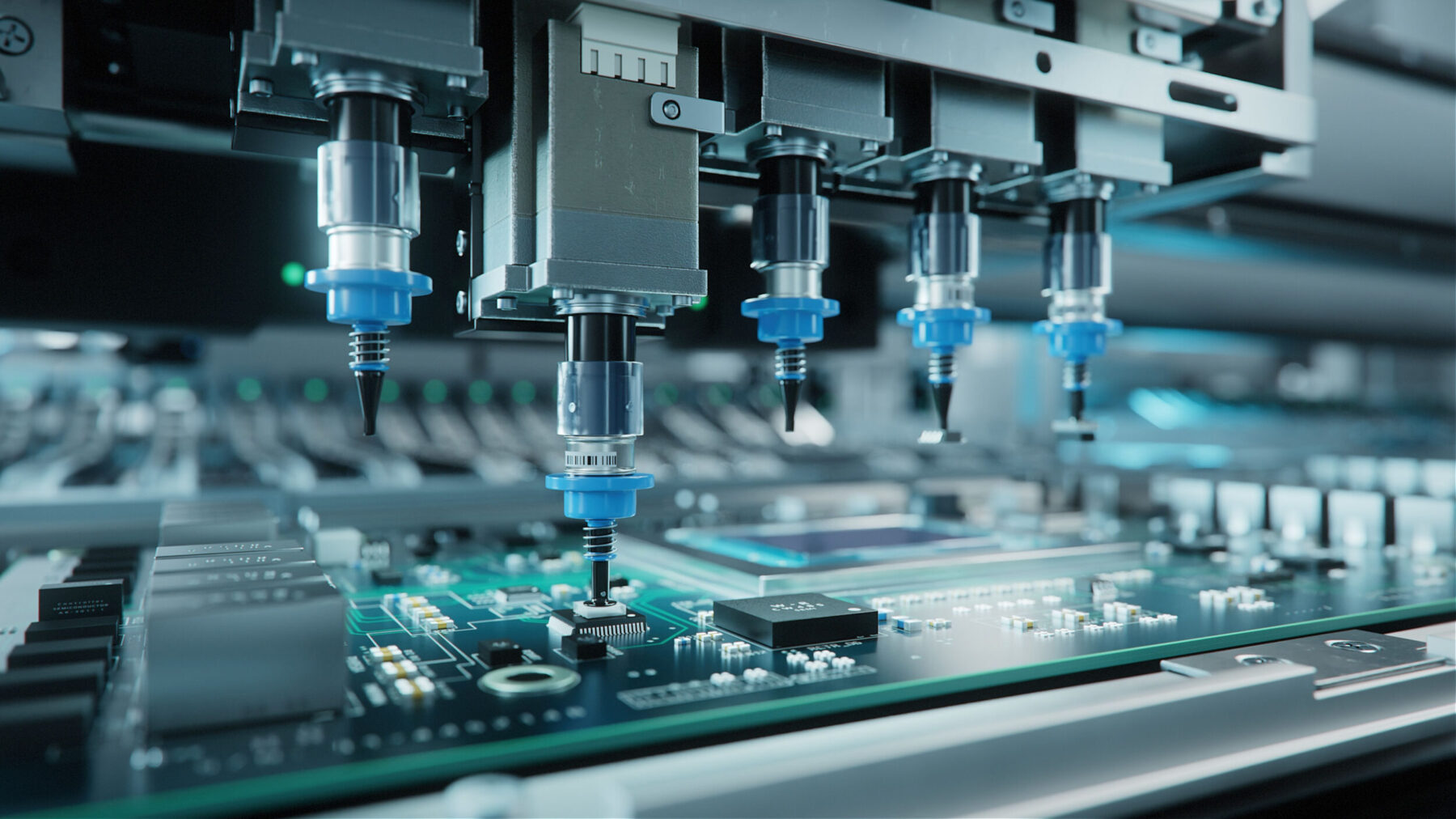
c. Component Placement
Automated pick-and-place machines then place the electronic components onto the board according to the placement files generated from the CAD design. This process requires high precision as components are often tiny and densely packed.
d. Reflow Soldering
The assembled PCBs are then passed through a reflow soldering oven. In this oven, the solder paste is melted, bonding the components to the board. The oven heats the board gradually to prevent thermal shock and ensure the solder joints are strong and reliable.
4. Testing and Quality Control
Quality control is critical in PCBA manufacturing. Automated optical inspection (AOI) and X-ray inspection are used to detect defects such as solder bridges or missing components. Functional testing verifies that the assembled board performs according to specifications.
5. Packaging and Shipping
Once tested and approved, the PCBAs are packaged and prepared for shipping to customers or to the next stage of assembly. The packaging is designed to protect the PCBAs from damage during transit.